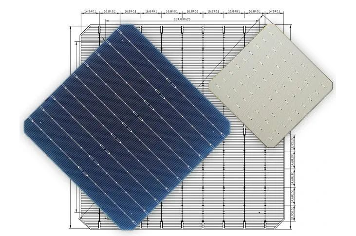
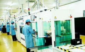
Battery sheet process flow:
Fleece (INTEX)→ diffusion (DIFF)→ post-cleaning (edging/PSG removal)→ anti-reflection film
plating (PECVD)→ Screen, sintering (PRINTER)→ Test, sorting (TESTER+SORTER)→ PACKING
1.Fleece
The purpose of velvet is to form a suede surface on the surface of the silicon wafer to reduce the
reflectivity of the battery, and the roughness of the suede can increase the secondary reflection
and change the light path and incident mode. Under normal circumstances, a pyramidal suede
can be obtained by treating single crystal with alkali; Treat polycrystals with acid, and you can get
wormhole shaped irregular suede. The treatment method is mainly different from that of single
polycrystal.
Process flow: fluting tank → washing → alkali washing → washing → pickling → washing
→ blow drying.
Under normal circumstances, silicon is considered to be non-reactive with HF and HNO3 (silicon
surface will be passivated). When present in a system of two mixed acids, the reaction of silicon
with the mixed solution is continuous.
2. Diffusion
Diffusion is the manufacture of the heart for the battery, is the manufacture of P-N junction for
the battery, POCl3 is the current phosphorus diffusion more choice. POCl3 is a l iquid phosphorus
source, and liquid phosphorus source diffusion has the advantages of high production efficiency,
good stability, uniform PN junction and good diffusion layer surface.
POCl3 decomposed into phosphorus pentachloride (PCl5) and phosphorus pentoxide (P2O5)
under the condition of more than 600℃, PCl5 has a corrosive effect on the surface of the silicon
wafer, when there is oxygen O2, PCl5 will decompose into P2O5 and release chlorine gas, so the
diffusion of nitrogen at the same time through a certain flow of oxygen. P2O5 reacts with silicon
at the diffusion temperature to generate silicon dioxide and phosphorus atoms, the generated
P2O5 deposited on the surface of the silicon and silicon continue to react to generate SiO2 and
phosphorus atoms, and form phosphate-silicon glass (PSG) on the surface of the silicon,
phosphorus atoms diffuse to silicon, the preparation of N-type semiconductor.
3. Etching
In the diffusion process, the back-to-back single-sided diffusion method is used, and the side and
back edges of the silicon wafer will inevitably be diffused with phosphorus atoms. When sunlight
hits the front of the P-N junction, the photogenerated electrons collected on the front of the P-N
junction flow to the back of the P-N junction along the phosphorus diffusion area of the edge,
causing a short circuit. The short-circuiting channel is equivalent to reducing the shunt resistance.
The etching process is to remove the phosphorus on the edge of the silicon wafer, avoiding the
short circuit of the P-N junction and resulting in the reduction of the parallel resistance.
Wet etching process: upper wafer → etching tank (H2SO4 HNO3 HF)→ water washing →
alkali tank (KOH)→ water washing →HF tank → water washing → lower wafer
HNO3 reaction oxidizes to SiO2, and HF removes SiO2. The role of the etching alkali tank is to
polish the unmade suede and make the battery smooth; The main solution of alkali tank is KOH;
H2SO4 is used to float the silicon wafers on the assembly line and does not participate in the
reaction.
Dry etching uses plasma to etch thin films. When the gas exists in the form of plasma, on the one
hand, the chemical activity of the gas in the plasma will become relatively strong, and the
suitable gas can make the silicon wafer react more quickly to achieve etching; On the other hand,
the electric field can be used to guide and accelerate the plasma, so that the plasma has a certain
energy. When bombarding the surface of the silicon wafer, the atoms of the silicon wafer material
are knocked out, which can achieve the purpose of using physical energy transfer to achieve
etching.
4.PECVD
Plasma chemical vapor deposition. The reflection loss rate of sunlight on the silicon surface is as
high as about 35%. Antireflection film can improve the absorption of sunlight by the battery, help
to improve the photogenerated current, and then improve the conversion efficiency: on the
other hand, the passivation of hydrogen in the film on the surface of the battery reduces the
surface recombination rate of the emission junction, reduces the dark current, improves the
open circuit voltage, and improves the photoelectric conversion efficiency. H can react with
defects or impurities in silicon, so as to transfer the energy band in the forbidden band to the
valence band or conduction band.
The silicon wafer is coated with a layer of SixNy film by conducting electricity to the graphite boat
under vacuum and at a temperature of 480 degrees Celsius.
5.Screen printing
In popular terms, it is to collect current for solar cells and manufacture electrodes, the first silver
electrode on the back and the second aluminum back field on the back of the printing and drying;
The printing of the third front silver electrode mainly monitors the wet weight after printing and
the width of the secondary grid line. If the second wet weight is too large, it will not only waste
the paste, but also may not be able to dry fully before entering the high temperature zone, or
even drive out all the organic matter in it so that the entire aluminum paste layer can not be
transformed into metal aluminum, in addition, the wet weight is too large may cause the battery
blade after sintering. If the wet weight is too small, all the aluminum paste will be consumed in
the subsequent sintering process to form a melting area with silicon, and the alloy area is not
suitable for contact as the back metal in terms of transverse conductivity or weldability, and there
may be bad appearance such as bulges. The width of the third grid line is too large, which will
reduce the light area of the battery and reduce the efficiency.
Printing method: physical printing, drying.
6. Sintering
Sintering is the electrode printed on the surface of the battery at high temperature sintering, so
that the electrode and the silicon wafer itself form ohmic contact, improve the open circuit
voltage and filling factor of the battery, so that the contact of the electrode has resistance
characteristics to achieve high conversion efficiency, sintering process can also facilitate the
introduction of PECVD process -H diffusion into the body, can play a good body passivation effect.
Sintering method: high temperature rapid sintering, heating method: infrared heating
Sintering is a set of diffusion, flow and physical and chemical reaction of a comprehensive effect
of a process, the front Ag through SiNH diffusion into silicon but can not reach the P-N surface,
the back Ag, Al diffusion into silicon, because the need to form alloys to a certain temperature,
Ag, Al and Si to form alloys stable and different, you need to set different temperatures to
achieve alloying.