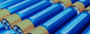
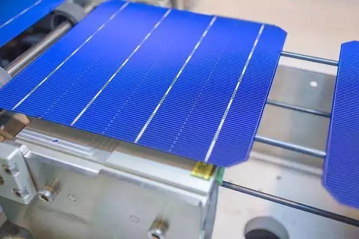
1, silicon wafer link: long crystal and slice as the core process link, “large size”, “lamination”, “N type” trend is clear
When the industrial silicon is purified, the silicon material that reaches the solar level quality standard is formed, which is used to prepare monocrystalline silicon and polysilicon according to the needs of the industry, and is respectively applied to the production of monocrystalline cells and polycrystalline cells. The preparation of silicon wafer mainly includes four links: long crystal, truncated square, slicing, test and sorting. Among them, long crystal and slicing are the core links. The monocrystalline silicon rod is prepared from polycrystalline silicon material by czochralysis or zone melting method; The preparation of monocrystalline silicon by ingot method refers to the preparation of monocrystalline silicon by a process similar to casting polysilicon, and the proportion of monocrystalline silicon sheets prepared by this process is still small. The most important trends in the silicon wafer segment include “large size”, “lamination” and “N-type”. Since 2018, the silicon size iteration has accelerated to drive a new round of equipment investment. According to CPIA data, the combined proportion of 182mm and 210mm sizes in 2021 has increased rapidly from 4.5% in 2020 to 45%, and it is expected that their proportion will continue to expand rapidly in the future. Due to the limited size of the device compatibility, the switch to 210mm size has released a large number of new equipment needs, significantly accelerating the equipment update. The trend of lamination is clear, and the industry side continues to promote. Lamination is conducive to reducing silicon consumption and wafer costs, but it will affect the fragmentation rate. At present, the slicing process can fully meet the needs of lamination, but the thickness of the silicon wafer should also meet the needs of the downstream battery and component manufacturing end. N-type monocrystal silicon wafer is the ideal material to achieve high efficiency solar cells, and the permeability is expected to continue to increase. N-type monocrystalline silicon has the advantages of less impurities, high purity, less minority carrier life, no grain boundary dislocation gap and easy to control resistivity, and is a high-quality material for the preparation of photovoltaic cells. In the case of the same metal impurity pollution, the surface recombination rate of N-type batteries is low, and the minority life is 1-2 orders of magnitude higher than that of P-type batteries, so under the same lighting conditions, the conversion efficiency is higher. In addition, because the N-type battery is a silicon substrate doped with phosphorus, there is no loss of boron-oxygen pair to form a composite center on the silicon substrate of the P-type battery, so the battery has almost no photoattenuation. As a whole, N-type cells produce at least 3 percent more electricity over their lifetime than P-type cells.”
2, the battery segment: the industrialization of high-efficiency batteries is further accelerated
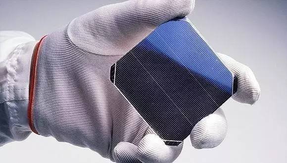
Crystalline silicon solar cells occupy about 95% of the share of solar cells, which is the highest level of industrialization and reliability of photovoltaic cells. At present, crystalline silicon cells are moving forward from the 2.5 era to the 3.0 era.
The first generation (2005 ~2018) conventional P-type battery: In 2020, the market share of traditional BSF battery (aluminum back field battery) has dropped to 8.8%, basically facing elimination.
The second generation (2016 ~ so far) PERC and PERC+ batteries: around 2016, with the outbreak of PERC battery industry acceptance, the industry has entered the 2.0 era. PERC batteries add back passivation and laser slotting on the basis of the traditional aluminum back field process. Further, on the PERC base, the PSG layer after diffusion is used as the phosphorus source, and the positive surface is secondary doped (phosphorus) by using the advantage of selective heating of laser, so as to form a selective heavy doped N++ layer. The introduction of SE technology makes the PERC battery further upgraded to PERC+, opening the 2.5 era and continuing to this day. At this stage, the industrialization of PERC+ battery is mature, and the conversion efficiency of the mass production line is about 23.0%~23.2%. On the other hand, it is also gradually approaching the upper limit of mass production conversion efficiency, and the industry has begun to explore the next generation of high-efficiency crystalline silicon solar cells.
The third generation (is opening large-scale industrialization) TOPCon, HJT, xBC and other high-efficiency batteries: on the one hand, based on the continuous pursuit of higher conversion efficiency, N-type batteries will gradually begin to replace P-type batteries, P-type batteries diffuse phosphorus to form N+/P structure, although the diffusion process is simple, but facing the conversion efficiency ceiling is low; N-type batteries diffuse boron to form P+/N structure, with the advantages of high minority life and matt attenuation. N-type battery representatives include TOPCon, HJT and so on. At the same time, there are still many players in the industry trying xBC batteries, by changing the battery structure to achieve efficiency improvement, P and N type xBC batteries are also actively moving towards mass production.”
3, component link: large silicon wafer to accelerate equipment updates, efficient batteries to promote demand change
Module production is the process of assembling cells and other raw materials into photovoltaic modules. The cells are pre-divided through the slicing process and welded with the interconnection strip to form a battery string. Then the battery string is connected with the bus belt to form a module string. Then the module string, glass, cut EVA and backplane are laid on top of each other. After lamination, trimming, framing, installation of cable box, silicone curing, surface cleaning, safety /EL/ testing, appearance inspection, packaging and other processes to form components. Among them, the series welding and laminating process is the more critical link in the production process of the component, and the corresponding equipment is the series welding machine and the laminating machine. The investment of component equipment is about 62 million yuan /GW, and the series welding machine accounts for about 35%. According to CPIA data, the investment of new component production line equipment in 2021 is about 62 million yuan /GW; In the value composition of component equipment, the value of string welding machine is higher, the single GW value usually exceeds 20 million yuan, accounting for about 35%, the value of laminating machine accounts for about 20%, and the value of automated production line and other equipment accounts for about 45%.
The demand for expansion of component links comes from:
1. the photovoltaic industry’s own high growth;
2. the rapid improvement of large-size permeability;
3.The new requirements of lamination for automation equipment;
4.The upgrade of the battery metallization realization method mainly affects the series welding machine and other links;
5.The diversity of battery technology routes. Large size and equipment compatibility: under the background of the rapid penetration of large silicon wafers, large-size high-power components are developing rapidly. Due to the incompatibility of equipment, an important driving force for the expansion of the industry from 2020 to 2021 comes from the replacement of large-size equipment for small-size.
According to PV infoLink statistics, by the end of 2021, there are more than 50 component enterprises with the production capacity of large-size high-power components, and the market share of large-size components will be close to 80% in 2022. Lamination puts new requirements on the automated production line of components: lamination can reduce the cost of silicon wafers, but it will also affect the fragmentation rate to a certain extent. At present, the average thickness of TOPCon cell N-type silicon wafer is 165μm, HJT is about 150μm, and IBC is about 130μm. The lamination trend puts forward new requirements for the automatic production line equipment at the component end. Looking forward to the future, the innovation of high-efficiency battery technology has spawned new demand for component equipment. Taking series welding as an example, there are differences in the structure and process of different high-efficiency batteries, and the series welding process needs to be adjusted. TOPCon battery, the conventional equipment can be compatible with TOPCon series welding, if the SMBB process is used, it needs to be upgraded to SMBB series welding machine. In terms of HJT battery, in order to maintain the electrical performance of the battery and protect the film layer, the HJT series welding machine needs to be customized to adapt to the low temperature process. After replacing amorphous silicon, the medium temperature above 300℃ can be used to reduce the difficulty of series welding; In addition, SmartWire series welding technology without main grid can also be used to replace the traditional series welding process. For xBC batteries, the battery is changed to the back contact structure, and the series welding process needs to be changed to one side welding. The conventional series welding machine is not compatible, and the xBC series welding machine needs to be replaced.”
If you have more needs, please contact us!